New Delhi: As we are moving toward a data-driven age, there is a need for faster and very low power computing. Memories play a crucial role in this, as for faster processing of data; the CPU rapidly reads and writes on the memory.
A researcher at the Indian Institute of Technology (IIT) Delhi has designed a device for high-density magnetic memory, in collaboration with the National University of Singapore(NUS).The proposed device may help reduce frequent charging of wireless electronic devices such as mobile phones and other Internet of Thing (IoT) based devices.
The main memory, i.e., the Random-access memory (RAM) is most commonly used in modern computer architecture. These are SRAMs and DRAMs, which are based on CMOS technology. They are fast but volatile and require a constant supply of power, which consumes lots of energy. But, if these could be made non-volatile, then computing could be made more energy-efficient.
Spintronics memories like spin-transfer torque magneto-resistive RAM (STT-MRAM) and spin-orbit torque magneto-resistive RAM (SOT-MRAM) are inherently non-volatile. They consume no power at standby. Also, their operation speeds are comparable to RAMs. Hence, these spintronics memories are the most potential candidates for replacing current electronic RAMs, says IIT Delhi statement.

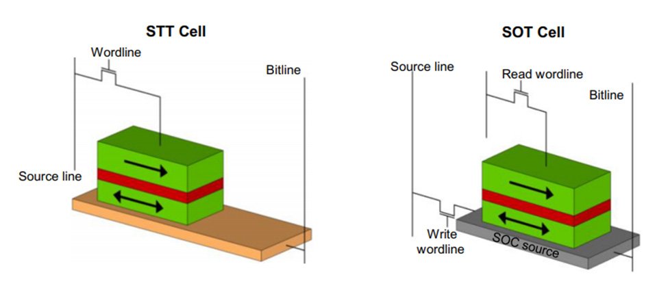
SOT-MRAMs are better than STT-MRAM in terms of reliability and writing speed but lags in achieving high integration density. This is because, unlike STT-MRAM, which is a two-terminal device and needs one transistor for reading and writing operation, the SOT-MRAMs require two transistors each for reading and writing. Thus SOT-MRAM requires a larger area per bit as compared to STT-MRAM, as shown in figure-1.
Also, SOT-MRAM is less prone to breakdown due to separate read and write paths, this is absent in STT-MRAMs. Hence, SOT-MRAM is the preferred choice among the research community however significant work is required to increase their areal density.
In a collaborative work between Prof. Rahul Mishra from the Centre for Applied Research in Electronics (CARE), IIT Delhi, and Prof. Hyunsoo Yang from the National University of Singapore(NUS) a possible solution for achieving higher integration density in SOT-MRAMs was proposed and experimentally demonstrated.
Prof. Rahul Mishra, CARE, IIT Delhi said, “We demonstrated a shared write channel based multibit SOT cell scheme, which reduces the number of transistors required per bit. This cell design requires half the area compared to conventional SOT MRAM, thus almost doubles the area efficiency of the memory chip”.

To make the above design feasible, the team designed a magnetic memory device, which can be programmed by the application of gate voltage. The gate voltage was used to migrate oxygen ions in the device, which resulted in modulation of the spin current polarity as shown in Figure 3. Thus, cells can now be written individually, and hence they obtained a full-fledged, working area-efficient SOT memory. The work was published in Physical Review applied journal.

Prof. Mishra further said, “The results of this work could eventually help to develop low power electronic devices. The frequent charging of wireless electronic devices such as mobile phones, IoT devices, etc would be significantly reduced with the proposed device. It would be especially useful for industrial applications where sensors are put in locations, which are not easy to access. Low power and high-density memory devices would not only help reduce global energy footprint but the saved energy can also be used for extra computational tasks”. (India Science Wire)


